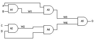
Introduction to VHDL

Introduction

VHDL was designed by the US Dept. of Defense in 1981 to describe the functionality of hardware systems. Today VHDL is one the two most widely used languages for hardware synthesis. VHDL is different from languages like C in that it is intended to describe hardware. A C program is usually compiled to a platform-specific assembly language and run as a binary. VHDL, on the other hand, is usually simulated using a simulator like Symphony EDA. In addition, synthesizable VHDL can be synthesized to hardware using a tool such as Synopsys and implemented on an FPGA. In this tutorial we will go over the basics of writing and testing VHDL programs.

Our First VHDL Design

entity AND2 is
port(  A,B: in bit;                                  -- A and B are inputs
       C: out bit);                                  -- C is the output
end AND2;     

architecture arch of AND2 is
begin
    C <= '1' when (A = '1' and B = '1') else '0';    -- C = 1 iff AB=1
end arch;
On the first line of our design we see the statement entity AND2. This is to specifiy that we are now working on a design that we are calling "AND2". Next you'll find a port statement. A and B are inputs to our design, and C is an output. The architecture statement says that we will now begin to specify the behaviour of our system. We want the output C to be '1' only when (A= '1' and B = '1'). Otherwise, C should take the value '0'. You can see that the output C takes the value of the logical AND of A and B. Here is a picture of the design we just described:

Structurally Connecting Components

Previously we created an AND2 entity in VHDL. Components can be combined to construct more complex circuits. Here is an example:

Here we have a circuit with five 2-input AND gates. Inputs are A,B,C,D and the output is O. Wires internal to the circuit are labeled W1,W2,W3,W4. It is possible to minimize this circuit, but suppose we wanted to implement the circuit in VHDL as-is. We can use five of our AND2 components to build this new circuit:
entity CIRCUIT is
port( A,B,C,D: in bit;           -- A,B,C,D are inputs
      O: out bit);               -- O is the output
      end CIRCUIT;

architecture str of CIRCUIT is

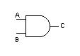
component AND2 is                -- This design will use our AND2 that
port(  A, B: in bit;             -- we wrote above. So we must include
       C: out bit);              -- it as a component.
end component;

signal W1,W2,W3,W4: bit;         -- signals W1-W4 represent internal
                                 -- wires to our circuit.
begin
  A1: AND2 port map(A,B,W1);     -- AND2 takes A,B, outputs W1
  A2: AND2 port map(C,D,W2);     -- AND2 takes C,D, outputs W2
  A3: AND2 port map(A,W1,W3);    -- AND2 takes A,W1, outputs W3
  A4: AND2 port map(W2,D,W4);    -- AND2 takes W2,D, outputs W4
  A5: AND2 port map(W3,W4,O);    -- AND2 takes W3,W4, outputs O
end str;
Our circuit has four inputs and a single output. Since we are reusing our AND2 entity, we must include it as a component. Then we create four signals, in this case they can be thought of as wires internal to our circuit. We place five seperate AND2 units in our circuit. The paramaters sent to each AND2 represent the inputs and output of each. For example, the input to A1 will be the A and B inputs, and the output will be W1. We can see that the circuit we created in VHDL mirrors the circuit in the image above.

Testing

How do we know that we described our hardware correctly? We could synthesize and download to an FPGA board, but there's a quicker way: We use software simulation. A testbench is a non-synthesible piece of VHDL code used for testing purposes. Here is a sample testbench for our AND2 entity:
entity AND2_test is                                                             -- test bench: no inputs or outputs
end AND2_test;
architecture tb of AND2_test is

  component AND2 is                                                             -- testing AND2 so must include 
  port(  A, B: in bit;                                                          -- as component
         C: out bit);
  end component; 
           
  signal X,Y,Z: bit;                                                            -- Signals to map to our AND2
  begin
    A1: AND2 port map(X,Y,Z);                                                   -- place AND2 with X,Y input
                                                                                -- and Z output
    process
    begin
    
      X <= '0';                                                                 -- set XY=00
      Y <= '0';
      wait for 10 ns;
      assert(Z='0') report "Error detected in Test Case 1!" severity warning;   -- make sure output is 0
    
      X <= '1';                                                                 -- set XY=11
      Y <= '1';
      wait for 10 ns;
      assert(Z='1') report "Error detected in Test Case 2!" severity warning;   -- make sure output is 1
    
      X <= '0';                                                                 -- set XY=01
      Y <= '1';
      wait for 10 ns;
      assert(Z='0') report "Error detected in Test Case 3!" severity warning;   -- make sure output is 0
    
      X <= '1';                                                                 -- set XY=10
      Y <= '0';
      wait for 10 ns;
      assert(Z='0') report "Error detected in Test Case 4!" severity warning;   -- make sure output is 0
    
      end process;
end tb;
Like most testbenches, our entity has no inputs or outputs. After we begin our architecture, there is a component AND2 statement followed by a list of inputs and outputs. If you look back to our AND2 design, you'll see that this is identical to our AND2 entity. The component statement exists to tell the entity that it will be using the AND2 component defined elsewhere, somewhat akin to a header file in C. With the AND2 port map(X,Y,Z) statement we create an instance of our AND2 design, mapping the signals X,Y,Z to A,B,C.

The idea behind testbenches is to feed some input into your circuit and then check the output against the known correct result. Here we do this by assigning X and Y and checking the Z output. First we set both X and Y to '0'. Then we check to make sure Z is equal to '0'(since 0 AND 0 = 0) with an assert statement. In this testbench we check all four possible input combinations against their known results to ensure correctness of our design.

In this case our circuit is correct, but what if it wasn't? If we tried to assert an output with a different value than what was generated by our design we'd get a severity warning from our simulator. This would probably be an indication that either or circuit doesn't work correctly. Also, a waveform output can be generated by simulator tools. These waveforms represent the values inputs and outputs take at different simulation times. Here is the output waveform from our testbench:

Library Operations

Every input, output and signal that we have seen so far has been of type bit. From now on we will not be using type bit since VHDL libraries exist that contain more flexible types with useful operations built-in. The std_logic type is what we will mostly be using from here on. To use the std_logic type, we must include two lines above our entity FOR EVERY ENTITY that is using std_logic. With std_logic we are able to do operations like AND, OR, and NOT without describing these gates directly like we did with AND2. Here is our circuit rewritten using std_logic operations:
library IEEE;                                           -- use the IEEE 1164 library
use IEEE.STD_LOGIC_1164.all;                            -- for std_logic

entity CIRCUIT is
port( A,B,C,D: in std_logic;                            -- inputs and outputs of type
      O: out std_logic);                                -- std_logic
      end CIRCUIT;

architecture bhv of CIRCUIT is
begin
  O <= (A AND (A AND B)) AND ((C AND D) AND D);      -- use AND operation directly
end bhv;                                                -- to produce output
Note the library and use statements right before the entity. These are necessary for any entity using type std_logic. We assign output O simply by using the AND operator for std_logic.

Here is a list of popular libraries that we will use, along with what functions they are commonly used for:

IEEE.STD_LOGIC_1164 - For use of std_logic and std_logic_vector. Will be used in nearly every VHDL entity you write.
IEEE.STD_LOGIC_arith - We will use this mainly for the adding and subtracting of std_logic_vectors. For example, if I had two four bit vectors v1 and v2 and wanted to add them into a third vector v3, I could simply write "v3 <= v1 + v2" if I included this library.
IEEE.STD_LOGIC_unsigned - Included when we want to use the type integer. Integers can be assigned decimal values, and can be converted to/from std_logic_vectors with the conv_integer and conv_std_logic_vector functions.
Useful Links
VHDL Language Tutorial
VHDL Tutorial: Learn by Example